9. The common base transistor
In this configuration the transistor has the base connected to a fixed voltage. The input signal arrives through the emitter of the transistor and the amplified signal exits through the collector of the transistor.
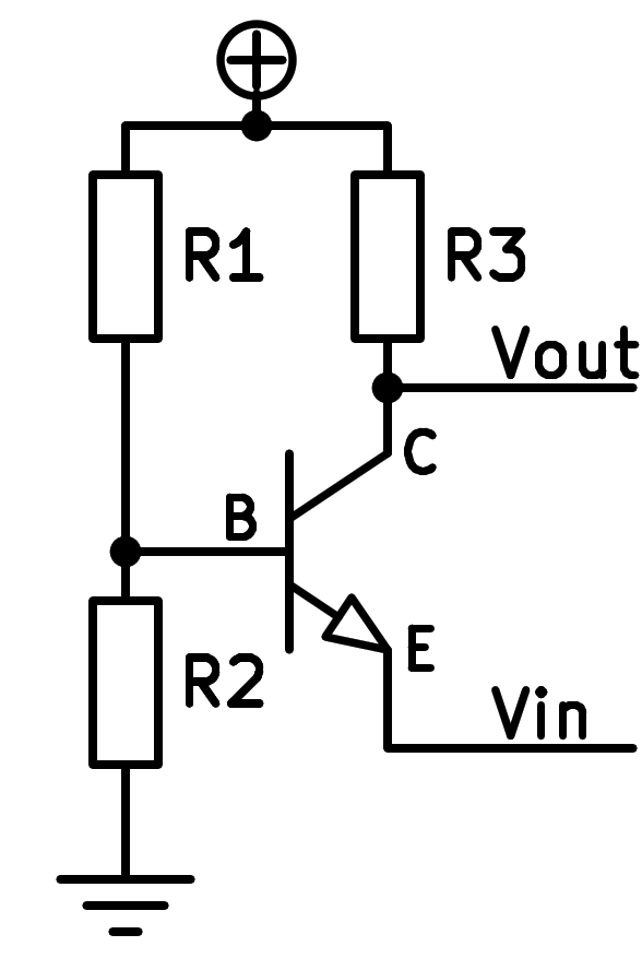
Simplified diagram of a common base NPN transistor.
This configuration allows the input voltage to be amplified while keeping the current the same. This operation is useful in signal input stages from a component that generates little voltage, but with relatively high currents.
An example of a practical application is to amplify the signal induced in a coil. For example, amplifying the sound picked up by a speaker, turning the speaker into a microphone.
Below you can see a simulation of an NPN transistor in common base configuration. The transistor amplifies a signal that enters through the emitter, generating a signal with much higher voltage that exits through the collector.
The function of each of the components is the following:
The alternating signal generator generates a small input signal of 0.050 volts peak.
Resistors R1 and R2 maintain a fixed voltage at the base that biases the transistor so that it always works with positive currents, despite the input voltage being both positive and negative.
The NPN transistor receives a small voltage signal through the emitter, which produces a current in the emitter. The transistor transfers that current from the emitter to the collector, where resistor R3 converts the current into a voltage higher than the input voltage.
At this stage there is no current amplification, only voltage amplification.
Resistor R3 receives the collector current and converts it into output voltage. The higher this resistance, the higher the output voltage and therefore the voltage amplification of the stage.
Exercises
Draw a simplified schematic of an NPN transistor working in common base configuration, showing where the input signal arrives and where the amplified signal leaves.
Draw a realistic schematic of an NPN transistor working in common base configuration.
What is the main function of a transistor operating in common base configuration?
What are resistors R1 and R2 for?
What is resistor R3 for?
What voltage gain does the simulated stage have?
To calculate the voltage gain, it is necessary to divide the voltage variation at the output by the voltage variation at the input.

You can obtain the necessary voltage values from the oscilloscopes located at the bottom of the simulator.
If we modify R3 with a value of 500 Ohm and R1 with a value of 8 kOhm, what happens to the output signal of the circuit? Why do you think this happens?