7. The common emitter transistor
In this configuration the transistor has the emitter connected to ground. The input signal arrives through the base of the transistor and the amplified signal exits through the collector of the transistor.
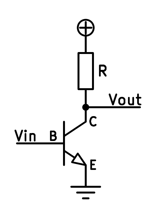
Simplified diagram of a common emitter NPN transistor.
This configuration allows both the input voltage and the input current to be amplified. This is useful in input and intermediate amplifier stages, where it is necessary to boost both the voltage and current of the input signal.
Below you can see a simulation of an NPN transistor in common emitter configuration. The transistor amplifies a small signal that enters through the base, generating a much larger signal that comes out through the collector.
The function of each of the components is the following:
The alternating signal generator generates a small input signal of 0.25 volts peak.
The function of resistor R1 is to limit the input current to a small value, which in this case varies between 40 and 80 microampere.
Resistor R2 adds a small direct current to the base so that the transistor can operate. This positive current that is added at the base is called bias current.
It must be taken into account that the transistor can only amplify positive currents, so it is necessary to add a small positive current to the input alternating current (positive and negative) for the transistor to work correctly.
The NPN transistor receives a small current through the base and amplifies that current so that it circulates, multiplied, through the collector.
Resistor R3 receives the collector current and converts it into output voltage.
About 100 times the current that flows through the base of the transistor will flow through this resistance.
Exercises
Draw a simplified schematic of an NPN transistor working in a common-emitter configuration, showing where the input signal arrives and where the amplified signal leaves.
Draw a realistic schematic of an NPN transistor working in common emitter configuration.
What is the main function of a transistor operating in common emitter configuration?
Modify the bias resistor R2 to be 40k. Draw the graph of the output voltage.
What happens to the output voltage when R2 is reduced?
Modify the bias resistor R2 to be 100k. Draw the graph of the output voltage.
What happens to the output voltage as R2 increases?
Modify the design of the common-emitter amplifier in the simulator so that it can amplify a 1-volt sine input signal to an output signal of at least 4 volts.
First it will be necessary to change the sine signal generator with the value of one volt.
Afterwards, the output resistance R3 must be modified to a smaller one so that the output signal varies by only 4 volts.
Finally, the bias resistor R2 must be modified so that the output signal is not clipped.
Take advantage of the signals from the right oscilloscope to guide you when modifying the resistor values.
Explain what resistor R3 is for. What happens if the resistance increases? What happens if the resistance decreases?