8. The common collector transistor
The common collector transistor is also commonly called emitter follower.
In this configuration the transistor has the collector connected to the positive voltage. The input signal arrives through the base of the transistor and the amplified signal exits through the emitter of the transistor.
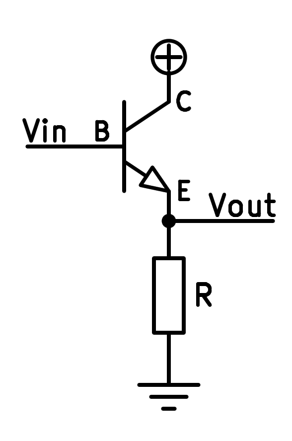
Simplified diagram of a common collector NPN transistor or also known as "emitter follower".
This configuration allows the input current to be amplified while maintaining the voltage unchanged. The output voltage, therefore, will be practically the same as the input voltage, minus the base-to-emitter diode voltage which is maintained at a value around 0.65 volts.
This operation is useful in the output stages of circuits, where a high current is necessary, for example, to drive a speaker.
Below you can see a simulation of an NPN transistor in common collector configuration. The transistor amplifies a signal that enters through the base, generating a signal with much higher current through the emitter.
The function of each of the components is the following:
The alternating signal generator generates an input signal (V_in) of 2 volts peak.
A direct voltage generator adds 4 Volts to the alternating voltage. It must be taken into account that the transistor can only amplify positive currents, so it is necessary to add an alternating positive voltage to avoid negative voltages.
The NPN transistor receives a voltage signal through the base with little current and maintains that same voltage at the emitter, minus a small voltage of 0.65 volts that always exists between base and emitter.
The current that arrives through the base is amplified so that it circulates, multiplied, through the collector and through the emitter.
Resistor R2 receives the current from the emitter and converts it into output voltage.
Exercises
Draw a simplified schematic of an NPN transistor working in a common collector configuration, showing where the input signal arrives and where the amplified signal leaves.
Draw a realistic schematic of an NPN transistor working in common collector configuration.
What is the main function of a transistor operating in common collector configuration?
Draw a graph with the generator voltage and the output voltage. What difference can you see between the graphs?
Modify the value of resistor R1 so that it is 20kOhm. Draw the graph of the output voltage.
What happens to the output voltage when resistance R1 increases?
In the simulator, increase the value of the output resistor R2 to 1000 Ohms.
What happens to the output voltage? What happens to the output current?