10. The Darlington scheme
The Darlington scheme is a device that combines two transistors connected in such a way that the emitter current of the first feeds the base current of the second as shown. you can see in the following image:
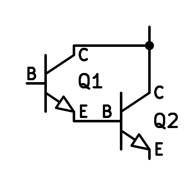
Schematic of two NPN transistors in Darlington assembly.
The Darlington scheme behaves like an ordinary transistor, with a collector, base and emitter.
- Advantages:
- The main advantage of this scheme is that the gain of the two transistors is multiplied, easily achieving very high gains, of several thousand. This allows high currents to be controlled with very small base currents.
- This scheme can be implemented with two discrete transistors connected or there are also integrated Darlington pairs in a single package, which reduces space.
- Disadvantages:
- The Darlington scheme has a slower response than a single transistor. This limits its operation as a switch to slow devices. To accelerate the shutdown of the second transistor, a resistor is usually placed between its base and its emitter.
- The minimum voltage between collector and emitter is greater than with a single transistor. This produces greater heating of the device when controlling the switching on and off of high current devices and produces an appreciable voltage loss.
- The voltage between base and emitter is higher, typically greater than 1.2 volts when adding two voltage drops of two transistors.
Simulation I
Below we can see the simulation of a Darlington scheme in common emitter configuration. This stage requires very little base current to power a 50 watt, 12 volt lamp.
This scheme can be used to drive high loads with low currents coming from digital control circuits, such as a microcontroller.
Simulation II
Below we can see the simulation of the output stage of a very popular oscillator circuit, the NE555. This output stage uses two Darlington configurations to amplify the circuit's internal signals and achieve high current to drive external loads.
In the upper box we can identify a Darlington scheme in common collector (collector connected to positive of the power supply). This scheme serves to feed the output with positive voltage.
In the lower box we can identify a common emitter Darlington scheme (emitter connected to the negative of the power supply). This scheme serves to feed the output with negative voltage.
This second lower box has some change compared to the standard configuration, by adding a 200 ohm resistor between the first transistor Q1 and the second transistor Q2. In addition, a diode is installed between the collectors of Q1 and Q2. These changes allow obtaining a lower voltage at the output than with the standard scheme.
The 200 ohm resistors on the right do not belong to the NE555 circuit, they are external load resistors.
Exercises
Draw a simplified schematic of two NPN transistors working in Darlington configuration.
Draw a realistic schematic of two NPN transistors working in common-emitter Darlington configuration.
Draw a realistic schematic of two NPN transistors working in common collector Darlington configuration.
What advantages does a Darlington scheme have over an individual transistor?
What disadvantages does a Darlington scheme have compared to an individual transistor? How can the effect of any of these drawbacks be reduced?
At the output stage of the NE555 circuit:
How many Darlington schemes can you identify?
What configuration is each one in and why?